Analog to digital conversion in almost all vision chips and APS is performed at the column or chip level. Incorporating ADC at the pixel level is very area consuming. However, for special applications, where the rate of data conversion and pixel read out is very high such an approach may prove beneficial [Fowler et al. 94, Fowler 95]. Although some disadvantages, such as the increased amount of data and the need for image reconstruction from the data, the introduction of high speed clocks running all across the chip, and the introduction of digital noise by these clock signals, can degrade the performance of this sensor.
In order to implement a feasible area efficient ADC for each pixel a one-bit first order delta-sigma ADC, shown in Figure 6.3, has been used in this sensor. The circuit simply tries to reduce the error between the analog output of the circuit and the input by averaging this error through a succession of clock cycles. The number of clock cycles required to achieve a desired signal-to-quantization noise ratio is given by [Fowler 95]:
![]()
Typically more than 60 clock cycles are required to achieve a SNR of around 50dB. This means that a large quantity of data is produced during a full ADC conversion. The actual image still needs to be reconstructed from the digital using a decimal filter.
The schematic diagram of the pixel circuit is shown in Figure 6.4.
A 64 ![]() 64 array of this circuit has been implemented in a 0.8
64 array of this circuit has been implemented in a 0.8 ![]() m 1P-3M CMOS process. Each pixel occupies an area of
m 1P-3M CMOS process. Each pixel occupies an area of ![]() . A redesign of this sensor uses multiplexed ADC for every four pixels,
and has 128
. A redesign of this sensor uses multiplexed ADC for every four pixels,
and has 128 ![]() 128 pixels each with an area of
128 pixels each with an area of ![]() [Yang
et al. 96].
[Yang
et al. 96].
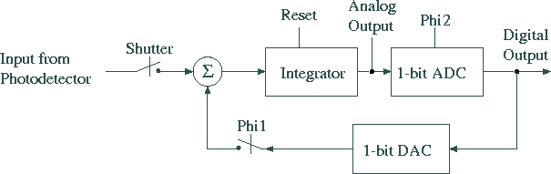
Figure 6.3: Block diagram of Fowler's pixel level first order
one-bit sigma-delta ADC. The clock rate of the Phi1 and Phi2
is much higher than the frame rate.
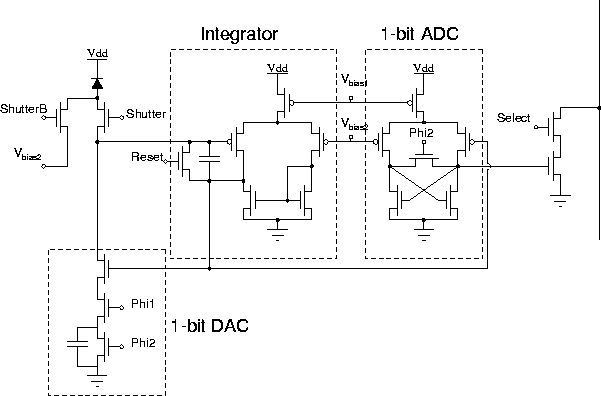
Figure 6.4: The schematic diagram of Fowler's pixel level ADC
sensor.
The
Image Sensor Group in Stanford.